Creating Nanostructures on Solid Surface Using Pulsed Laser
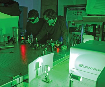
"We are using intensive pulsed lasers to study interactions between laser pulses and matter for potential applications in nanoscience and nanotechnology." says Assoc. Prof. Mengyan Shen, head of the Lab's Femtosecond Laser Group. The team utilizes femtosecond pulsed lasers at 400 and 800 nanometers (nm) to fabricate nanostructures on a solid surface.
"The technique is highly efficient because it id deferral orders faster yarn electron-beam writing and ion-beam etching, and is applicable to different materials," he say. "It has applications in opto-electronics such as high-efficiency photodetectors and solar cells, as well as in biology and medical research such as micro/nano tunnels for low-friction fluidity, and nanostructured metal surfaces for other applications."
The group has successfully developed soft nanolithigraphy to three-dimensionally replicate silicon nanospike structures made by femtosecond laser pule irradiation to a precision of 5nm. The replicated nanostructures are being used to manufacture identical chemical and gas sensors at very low cost. This research had been supported by the National Science Foundation (NSF)
"With metal nanostructures formed with femtosecond laser irradiation, a natural-like photosynthesis has shown great potential for storing solar energy and saving out environment," says Shen. This research has been partially supported by seed fund from the NSF Center for High-Rate Nanomanufacturing at UMass Lowell
He says the group is also developing techniques for time-resolved spectra measurements, in the time range from seconds to femtoseconds, for other applications in nanoscience and nanotechnology.
Read more about the research (pdfs)
Technology Used to Store Solar Energy